◆ 1. Automation function
Highly integrated automation functions pursue high-efficiency testing
Reduce human operation error in detection
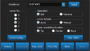
4 inch automatic motor table Automatic cantilever replacement function
◆ 2. Reliability
Eliminate errors caused by mechanical causes
image.png Large-scale horizontal scan
Atomic force microscopes using tube scanners usually obtain plane data through software correction methods for the curved surfaces generated by the arc motion of the scanner. However, the software correction method cannot completely eliminate the influence of the arc movement of the scanner, and the distortion effect often occurs on the picture.
AFM5500M is equipped with a newly developed horizontal scanner, which can realize accurate testing without being affected by circular arc movement.
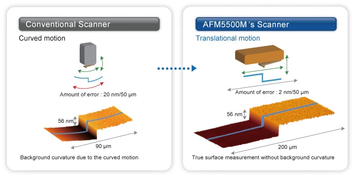
Sample :Amorphous silicon thin film on a silicon substrate
image.png High-precision angle measurement
The scanner used in an ordinary atomic force microscope will bend (crosstalk) when it stretches vertically. This is the direct cause of the topography error of the image in the horizontal direction.
The new scanner mounted in the AFM5500M will not bend (crosstalk) in the vertical direction, and can get correct images without distortion in the horizontal direction.
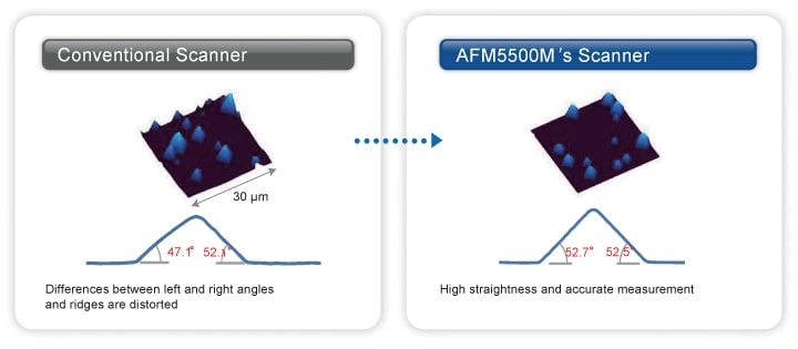
Sample : Textured-structure solar battery(having symmetrical structure due to its crystal orientation.)
* 使用AFM5100N(开环控制)时
◆ 3. Integration
Intimate integration with other detection and analysis methods
Through the SEM-AFM shared coordinate sample stage, the surface morphology, structure, composition, physical properties, etc. of the sample can be quickly observed and analyzed in the same field of view.
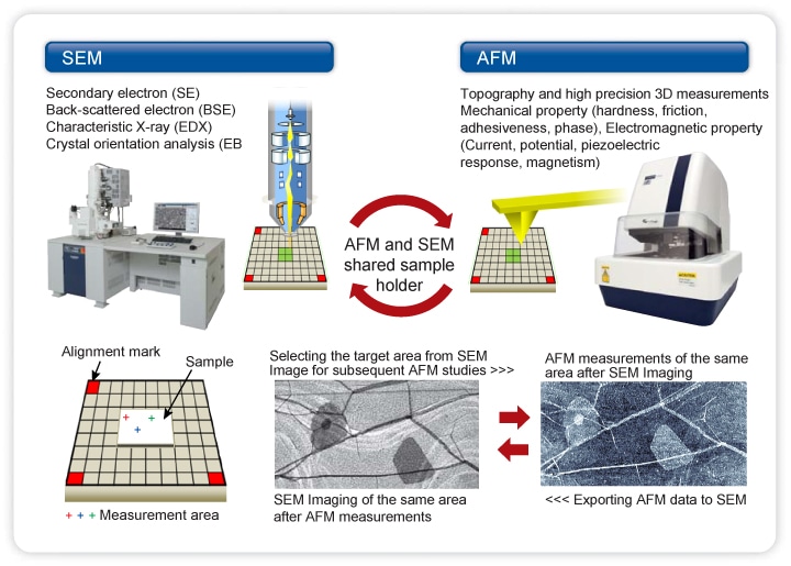
SEM-AFM observation example in the same field of view (sample: graphene/SiO2)
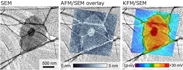
The ovrlay images createed by using AZblend Ver.2.1, ASTRON Inc.
The image above is the application data of the shape image (AFM image) and potential image (KFM image) taken by AFM5500M and superimposed on the SEM image respectively.
image.png It can be judged by analyzing the AFM image that the SEM contrast characterizes the thickness of the graphene layer.
image.png The difference in the number of graphene layers results in the contrast of the surface potential (work function).
image.png The contrast of SEM images is different. The reason can be found through SPM's high-precision 3D topography measurement and physical characteristics analysis.
In the future, it is planned to be used in conjunction with other microscopes and analytical instruments.
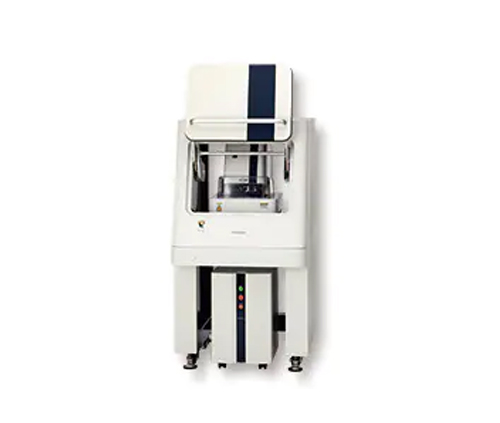
AFM5500M host
* Parameters are related to equipment configuration and placement environment.
AFM5500M dedicated atomic force microscope workstation
* WINDOWS is a registered trademark of Microsoft Corporation in the United States and other countries.
* RealTune is a registered trademark of Hitachi High-Technologies Corporation in Japan, the United States and Europe.
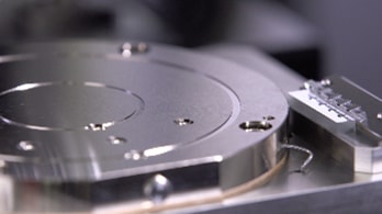
Optional items: SEM-AFM combined system