
In recent years, Suzhou Industrial Park has focused on the technological leapfrogging plan and the goal of creating a first-class innovation park. It has invested more than 500 million yuan in key industries such as software, integrated circuits, biomedicine, animation and games, nanotechnology, and next-generation communications. Focus on building more than 20 science and technology public service platforms and more than 30 open laboratories.
For this reason, the park has specially established three major public service systems with a scientific and technological public service platform collaboration and sharing network as a link, forming a public technology service platform, an open laboratory, and an entrepreneurial support service platform.
In order to further increase the influence of various platform institutions and promote them to better serve enterprises, we will conscientiously implement the "3+5" transformation and upgrading industry development plan, and focus on leading industries such as electronic information manufacturing, machinery manufacturing, and modern service industries. Be bigger and stronger, and focus on cultivating five emerging industries, including biomedicine, nano-photoelectric new energy, software and animation games, integrated communications, and environmental protection. This publication, together with the Park Science and Technology Development Bureau and the SME Service Center, launched the "Suzhou Industrial Park Public Platform Equipment Series Tour".
Can see one-hundred-thousandths of a strand of hair
"I heard that the analysis of chemical substances can clearly see the atoms of the substance, and the failure analysis only needs a glance to know the reason." Is this really magical? With questions and curiosity, we visited the electron microscope laboratory of the test and analysis platform of the Suzhou Institute of Nanotechnology, Chinese Academy of Sciences under the leadership of Professor Zhang Jinping, the director of the scanning electron microscope laboratory.
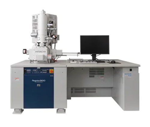
Under Professor Zhang’s patient introduction and on-site demonstration, we learned that it is the field emission transmission electron microscope (Tecnai G2 F20 S-TWIN TEM), which is located on the first floor of the Nano Institute, that can image the atom. The rate is as high as 0.2 nanometers, which is only twice the diameter of a small hydrogen atom, which is equivalent to one-300,000th of the diameter of a human hair, so that the structure and chemical composition of substances can be analyzed on the atomic scale, so that customers can By observing and analyzing the morphology and composition of the substance at the nanometer level, it can be seen at a glance whether the substance is qualified, and the failure analysis of the substance can be carried out. "Of course, in addition to analyzing the reasons for failure, some companies can image very well done samples at the atomic level and can also be used as advertising photos," Professor Zhang joked. According to reports, the electron microscope is currently the world's first-class electron microscope, which basically represents the new level of electron microscopy in the world today. "Why do companies have to use electron microscopes of up to several million to analyze substances at the nanometer level? Many optical microscopes on the market only need tens of thousands or even a few thousand, and the resolution can be 100 nanometers?" I wondered. . "Take this carbon nanotube as an example. It is now widely used. Composite materials, electronic devices, batteries, supercapacitors, and military bulletproof vests are all used. Its strength is 100 times that of steel, and its density is only that of steel. 1/6, some people say that if you build a ladder between the earth and the moon, only carbon nanotubes can take on this big task." Professor Zhang pointed to a carbon nanotube imaged under an electron microscope (with picture) and continued with a smile Said, "Look, we can clearly see that there is a bad combination in our nano-level imaging, but it is completely invisible under a low-resolution optical microscope. I thought it was a perfect sample. Woolen cloth. "
The laboratory is equipped with super hardware and software equipment
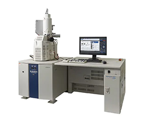
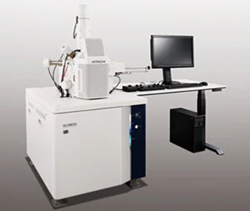
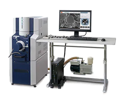
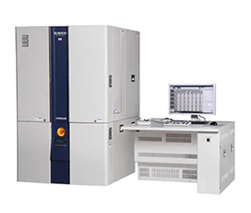
The leaders of the institute have paid great attention and attention to the construction of the test and analysis platform, and allocated 40 million yuan in the preparation of funds for the purchase of equipment. In the past two years, nearly 10 million yuan has been invested in various projects. The total equipment investment has reached about 5,000. 10,000 yuan, of which the electron microscope laboratory invested more than 20 million yuan. The laboratory has first-class hardware facilities. In addition to the field emission transmission electron microscope, there is also a thermal field emission environment scanning electron microscope and a Hitachi cold field high resolution transmission electron microscope , A tungsten filament scanning electron microscope, a MonoCL3+ cathodoluminescence spectrometer (with a liquid nitrogen cooling stage and a liquid helium cooling stage), a set of SmartEBIC electron beam induced induced current device and a complete set of electron microscope sample preparation equipment. These equipment are in physical Science, materials science, chemistry and biology have a wide range of applications. From semiconductor devices, luminescent materials, organic conductive materials, and even biological samples, it can provide nano- or atomic-scale high-resolution images, chemical element distribution maps, and interface structures. , Phase analysis and other results, and especially suitable for the anatomical analysis of nano devices and new materials.
Professor Zhang Jinping, the director of the laboratory, studied under the founders of Chinese electron microscopes, Academician Guo Kengxin and Academician Ye Hengqiang. He is one of the doctors in electron microscopy cultivated in my country. He has been engaged in electron microscope research in the United States for 20 years and is in the field of electron microscopy analysis. He has a high reputation. He has worked in the California Nano Center and has cooperated with many cutting-edge laboratories in the nanomaterials industry, including Dr. H. Kroto (Nobel Prize winner in 1996, discoverer of C60) and so on. He is also the current chairman of the Guo Kexin Foundation. Since the laboratory’s formal operation in 2009, it has served a number of users outside the office, including Sony Suzhou R&D Department, Sujing Group, Shanghai Silicate Institute, etc., totaling more than 30. Among them, enterprise users account for two-thirds of outside users. The average service time has reached 10 hours, and the existing equipment has basically reached full capacity. In addition, the laboratory has provided electron microscopy services for the University of California, Santa Barbara, Santiago, the Technical University of Munich, Taiwan University, etc., and trained scanning electron microscope operators. After just one year, the electron microscope room A professional team that can provide the above-mentioned project services has been formed, and can provide enterprises with a one-stop service from electron microscope sample preparation to data analysis.
During the visit, Professor Zhang pointed to a staff member who was operating the electron microscope and said: “This is a commissioned company’s own employees. We welcome the company’s staff to test by themselves. After a few hours of training, they can completely operate it by themselves. In addition, in the second phase of the construction of the Suzhou Institute of Nanotechnology, it is planned to expand to the total number of eight electron microscopes and have complete and advanced sample preparation equipment; cultivate a group of high-level electron microscope professionals within three to five years; operating mechanism A breakthrough has been made in this field, and it has developed into an electron microscope center that is full of vitality, has core values for the industry, and has an important supporting role for cutting-edge scientific research."