
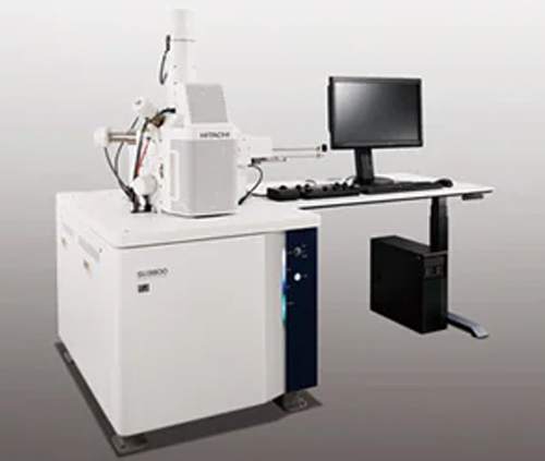
①SU3900 is equipped with a multi-functional super large sample bin as standard, which can handle the observation of large samples
■The sample stage can carry oversize/overweight samples
By changing the sample prompt, it can prevent damage to the equipment or sample due to contact with the sample
Optional sample exchange compartment, which can quickly change samples while maintaining a vacuum in the main sample compartment, greatly improving work efficiency
Equipped with the function of removing the restriction on the movement of the sample stage, which improves the degree of freedom*
Infrared CCD detector improves the safety of the sample stage movement
■Support full field of view movement. SEM MAP supports full-field observation of large samples
Combined with GUI, can be equipped with sample chamber navigation camera
Cover the entire observable area
Support 360 degree rotation
②With the enhancement of various automation functions, the operating performance has been further optimized.
■Simple GUI that can be easily operated with a mouse
■Various automation functions
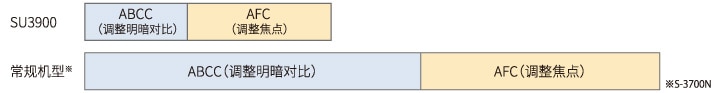
After the automatic adjustment algorithm is improved, the waiting time is reduced to less than 1/3 of the previous (※S-3700N ratio)
Improved auto focus accuracy
Equipped with Intelligent Filament Technology (IFT)
■Multi Zigzag, can realize multi-area wide-field observation
■Report Creator, can use the obtained data to generate data reports in batches
③Provide application solutions that meet test requirements
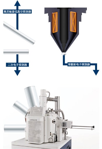
■Detectors that can meet a variety of observation needs
Equipped with high-sensitivity UVD*, support CL observation
High-sensitivity semiconductor backscattered electron detector, switching component/concave and other images
■Equipped with a multi-functional large sample compartment, which can carry a variety of accessories
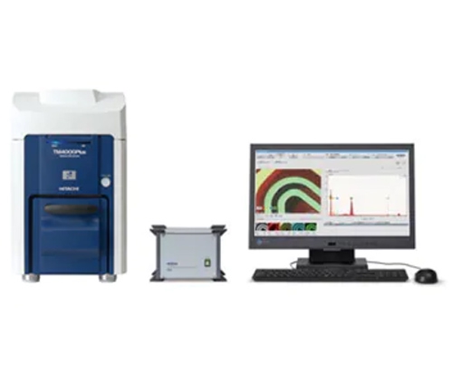
>■SEM/EDS integration function*
■Three-dimensional display measurement software Hitachi Map 3D*
■Support image measurement software Image pro
*Accessories


* 1.指正放大倍率为127 mm x 95 mm(4x5照片尺寸)的显示尺寸。
* 2.指定放大倍率为509.8 mm x 286.7 mm(1,920 x 1,080像素)的显示尺寸。
◆ ①The standard multi-function super large sample warehouse supports the analysis of large samples
■The sample stage can carry oversize/overweight samples
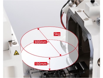
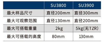
image.png By changing the sample prompt, you can prevent damage to the equipment or sample due to contact with the sample
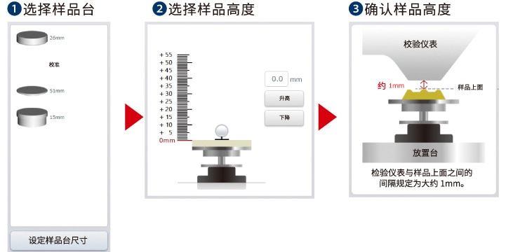
The operation steps for replacing the sample are displayed on the GUI. It can avoid sample contamination or damage due to human misoperation. Even samples with uneven heights that are difficult to detect or oversized samples can be easily replaced.
Sample exchange warehouse*
Optional sample exchange compartment, which can quickly change samples while maintaining a vacuum in the main sample compartment, greatly improving work efficiency

Equipped with the function of removing the restriction on the movement of the sample stage, which improves the degree of freedom*
SU3800 / SU3900 is equipped with the sample stage free mode, which opens up the freedom of sample stage movement. The operator can judge by himself and move the sample table freely.
※When selecting the free mode of the sample stage, please also select an infrared CCD detector.
image.png Infrared CCD detector*, which improves the safety of the movement of the sample stage
The infrared CCD detector is a device used to monitor the inside of the sample chamber. By using an infrared camera, you can monitor the inside of the sample chamber while observing the SEM image. In order to obtain a more detailed position, zoom in on the CCD image and move the observation position.
*Accessories
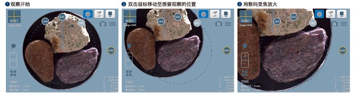
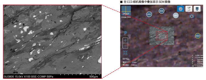
■Support full-field movement, SEM MAP supports full-field observation of large samples
image.png Combined with GUI, can be equipped with sample chamber navigation camera
The SEM MAP combined with GUI realizes the wide-angle camera navigation function because of the use of the sample chamber navigation camera. Specify the observation target position on the SEM MAP, and you can smoothly move to any specified position. Using the image or external image taken by the camera navigation system with a wide field of view, by freely zooming in or zooming out the image, you can switch the color image of the large field of view to a high-magnification SEM image.
*
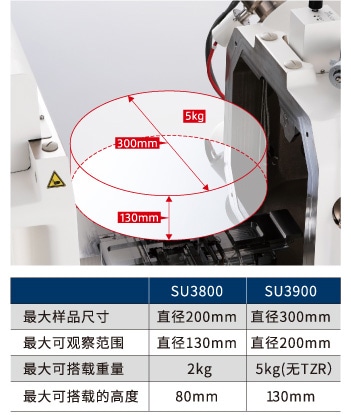
Cover the entire observable area
The camera navigation system can realize a large field of view SEM MAP observation through the image stitching function. The observation area is 130mm in diameter (SU3800)/200mm in diameter (SU3900), and can be linked with the sample stage R to move to the largest observation area for large samples.
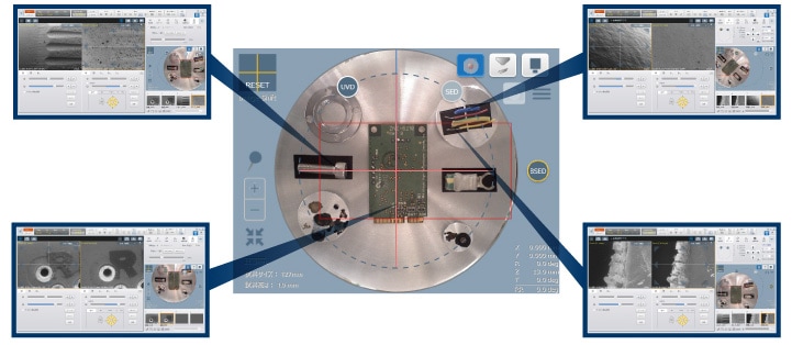
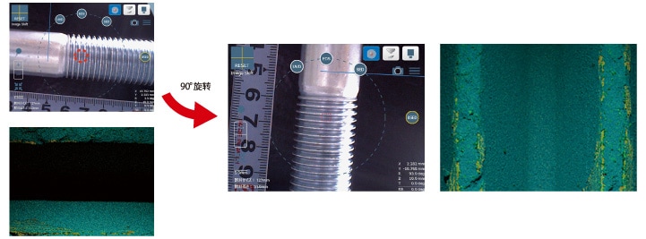
image.png supports 360 degree rotation
The SEM MAP operation interface can intuitively display the position relationship between the sample and the detector. Therefore, when observing samples with large height differences, the sample stage or electron beam can be rotated as required to obtain the best observation and analysis position to avoid the shadow effect. .
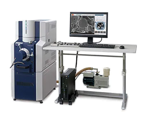
◆ ②With the enhancement of various automation functions, the operating performance has been further optimized.
■Simple GUI that can be easily operated with a mouse
Equipped with a simple UI, simple operation, as intuitive as a touch screen.
image.png From moving the sample stage to the sample observation, just click the mouse to achieve
image.png can also be operated on touch screen
image.png The main window is a large 1280x960 pixel window
image.png You can switch the display mode, and display/shoot two different signals at the same time
■Various automation functions
image.png After the improvement of the automatic adjustment algorithm, the waiting time is reduced to less than 1/3 of the previous (※S-3700N ratio)
After the sample is installed, the image is adjusted through automatic light path adjustment and various automatic functions, and then the sample image can be obtained immediately. The highly automated function adopts a newly designed calculation program, and when the automatic image adjustment function is executed, the waiting time is reduced to less than 1/3 of the previous one.
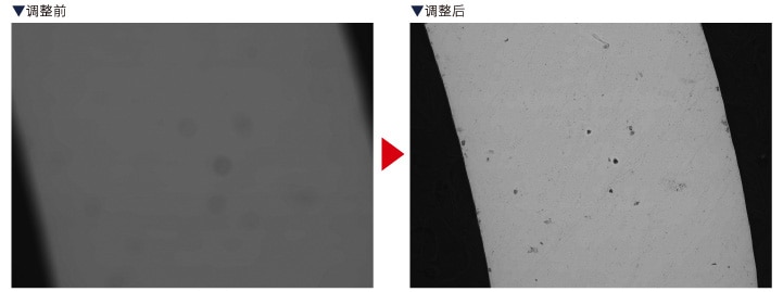
A new algorithm is used to improve the accuracy of auto focus
The newly upgraded auto-focus adjustment function can easily obtain good images even for smooth samples that were difficult to adjust in the past.
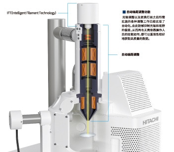
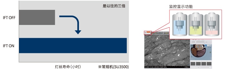
Equipped with Intelligent Filament Technology (IFT)
Automatically monitor the status of the filament, and automatically control to keep it in the best performance state.
Equipped with a display that shows the time of filament replacement.
With this function, large-scale analysis such as long-term continuous observation and data analysis that were difficult to handle can be realized with peace of mind.
■Multi Zigzag*, can realize multi-area wide-field observation
Multi Zigzag can automatically acquire a continuous field of view. You can shoot multiple high-magnification images in different fields of view, and use the Viewer function to stitch the captured images to create a large field of view image.
*Accessories
Report Creator, can use the obtained data to generate data reports in batches
In Report Creator, the collected images such as SEM images, EDS data and CCD camera images can be unified and integrated to generate reports. The created report can be saved in Microsoft Office® format. The saved file can be edited through Microsoft Office®.
◆ 矿物的观察分析案列
显示了锆石晶体在相同视野下的观察结果。在BSE图像中很难看清铬浓度的缓和偏差。但是,在CL图像中可以确认到暗 色区域是对应于错浓度较高的区域。

◆ 金属材料

◆ 陶瓷材料

◆ 电子零件

◆ 生物/医药品