
◆ Core Concept
1. High-performance SEM lens barrel equipped with two lens modes
image.png High resolution observation can be achieved in HR mode (half inner lens)
image.png High-precision machining endpoint detection can be achieved in FF mode (Timesharing Mode)
2. High throughput processing
image.png High current density FIB can achieve rapid processing (beam current 100nA)
image.png Users can set the processing steps according to their own needs
3. Micro Sampling System*3
image.png Use ACE technology (processing position adjustment) to suppress the Curtaining effect
image.png Control the incident angle of the ion beam to prepare thin film samples with uniform thickness
4. Triple Beam System*3 that realizes low damage processing
image.png Using low acceleration (Ar/Xe) ion beam to achieve low damage processing
image.png Removal of gallium pollution
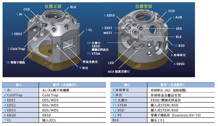
5. The sample chamber and sample stage are suitable for various sample analysis
image.png Multi-interface sample compartment (small and small interfaces)
image.png Large anti-vibration sample stage (150 mm□)
*3 optional
◆ High-performance SEM lens barrel
The SEM equipped with Ethos is equipped with two lens modes. The HR mode can place the sample in the lens magnetic field to achieve high-resolution observation of the sample. FF mode can switch between FIB irradiation and SEM observation in the shortest 10nsec. Users can perform FIB processing while observing SEM images at a high-speed frame rate. Therefore, they can easily determine the processing end point of the cross-section. NX5000 adopts electromagnetic compound lens, which can maintain high-resolution observation even in FF mode.
◆ High-resolution SEM observation example
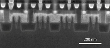
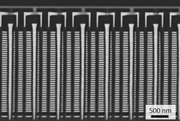
Fin-FET 14 nm device 3D-NAND device
◆ High-performance FIB lens barrel
High current density FIB can realize rapid processing, wide area processing, multiple automatic processing, etc.
◆ Time-sharing scan mode
When FIB, Ar/Xe ion beam is irradiated, SEM images can be observed in real time or time-sharing
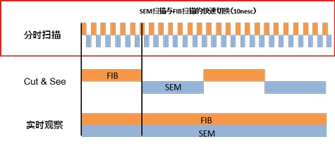
■ Time-sharing scan mode can stop processing at the most appropriate position
■ Cut & See mode can realize high-resolution SEM observation
■ Real-time processing mode is FIB processing mode with priority on processing time
◆ Use Cut & See mode to realize 3D reconstruction
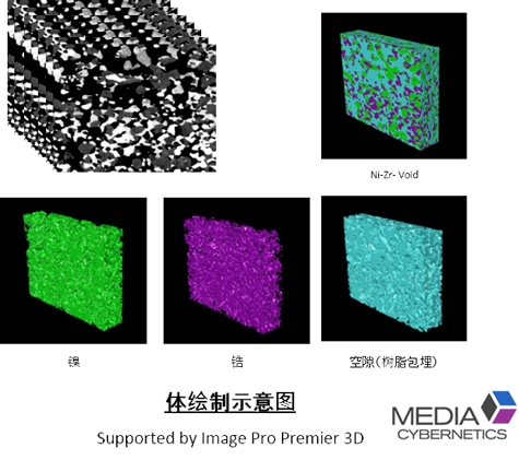
FOV:20 μm
Cut & See:200 sheets
Slice pitch:20 nm
SEM acceleration voltage: 1.5 kV
Fuel electrode of solid oxide fuel cell (Ni-YSZ)
Sample provided: Institute of Production Technology, University of Tokyo
Professor Naotake Shikaen
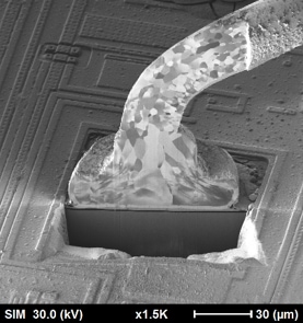
◆ High-quality TEM sample preparation to suppress FIB processing damage
Using low acceleration argon ion beam and high current density FIB, it can realize rapid processing, wide area processing and multiple automatic processing.
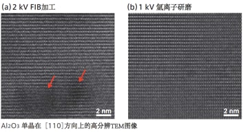
When performing FIB processing at a low acceleration voltage of 2kV, observe the sample damage caused by Ga+ ion irradiation (red arrow) (Figure a)
Then, argon ion milling was performed at a low acceleration voltage of 1kV to eliminate the damage layer caused by FIB processing, and the lattice image can be clearly observed.
Triple Beam System (Argon/Xenon)

When preparing extremely thin samples, a wide-area and low-damage processing method must be used.
Ethos adopts the ACE technology that combines sample processing position adjustment and low acceleration argon ion beam finishing to prepare high-quality TEM film samples.
ACE: Anti Curtaining Effect
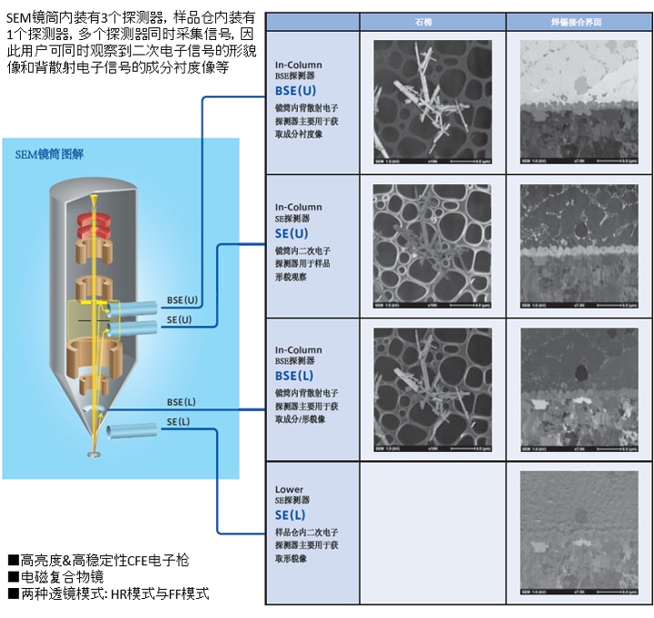
◆ GUI design further improves visual beauty and response speed
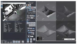
4 kinds of signals to choose from
■ The In-Column detector (SED×1, BSE×2) and the SE detector in the sample chamber can collect signals at the same time
■ Equipped with beam condition saving and reading function of each SEM optical system
■ The most suitable detector can be selected according to different observation requirements (shape/composition)
■ Each detector can realize individual settings, storage and output such as contrast and brightness
◆ Establish diversified processing modes and sequencing
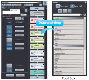
Register and output various processing modes/observation conditions
■ Drag and drop to easily establish processing/observation sequence
■ Each processing mode and program processing can be freely edited and registered
■ You can simply complete the processing settings by outputting the current program processing
■ It can greatly simplify repeated operations by reading the current sequence
■ You can copy and edit the sequence to further improve scalability and flexibility
Through the use of various processing modes, the processing range can be flexibly set
■ Processing mode supports rectangle, circle, triangle, parallelogram, oblique processing, Bit-map processing, etc.
■ Application processing supports cross-section processing and TEM sample preparation
■ Vector Scan*3 can display the processing range based on vector information to complete precise positioning. Moreover, after the image (bmp) is converted into a vector, the sample processing can also be continued
■ Equipped with various ion beam irradiation position compensation functions (drift correction function), enabling high-precision machining
*3 optional
◆ Large sample warehouse supports various uses
■ Equipped with anti-vibration sample stage supporting high-resolution observation
■ Set up a variety of interfaces, you can install more optional accessories, to achieve a variety of sample processing, observation and analysis