

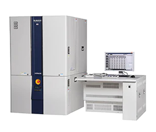
Specially designed for high-resolution imaging of electron beam sensitive samples and advanced semiconductor devices that require 3 million times stable observation.
image.png The new electron gun and electron optical design improve the low acceleration voltage performance.
0.4 nm / 30 kV (SE)
1.2 nm / 1 kV (SE)
0.34 nm / 30 kV (STEM)
image.png Use improved high vacuum performance and unparalleled electron beam stability to achieve high-efficiency cross-sectional observation.
image.png The newly designed Super E x B energy filtering technology is used to efficiently and flexibly collect SE/BSE/STEM signals.