
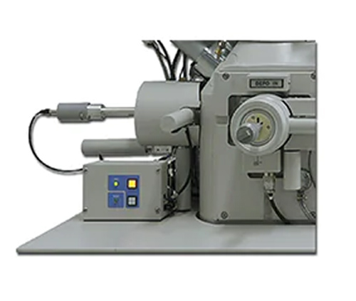
◆ Focused ion beam (FIB) micro-sampling device and focused ion beam (FIB) micro-sampling method
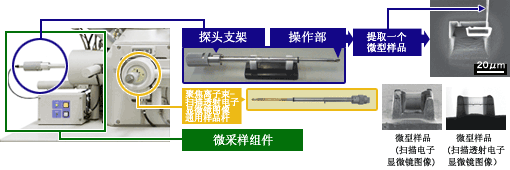
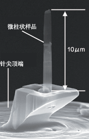
◆ Focused ion beam (FIB) micro-column sample preparation example
A micro-pillar sample contains an analysis point that is accurately cut directly from the semiconductor device. Change the direction of the incident focused ion beam (FIB) to cut or process the micro-sample into any shape.
◆ Focused ion beam-scanning transmission electron microscope system
The newly developed semiconductor device evaluation system consists of the FB2200 focused ion beam (FIB) system and the HD-2700 200 kV (STEM) scanning transmission electron microscope. From searching for material defects (organizations) to high-precision structure analysis of sub-nano thin films, it only takes a few hours to complete.
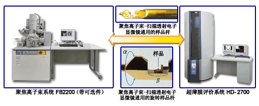
Focused ion beam-transmission electron microscope (scanning transmission electron microscope) (FIB-TEM (STEM)) sample rods are interchangeable and shared
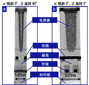
◆ DRAM observation example
SEM image of the micro-columnar sample at the tip of the tip Bright-field STEM image of the micro-column sample
徐州Oxford Instruments Xplore Energy Spectrum Detector
徐州Spherical aberration field emission transmission electron microscope HF5000
徐州TM series dedicated energy spectrometer (EDS) AZtec series
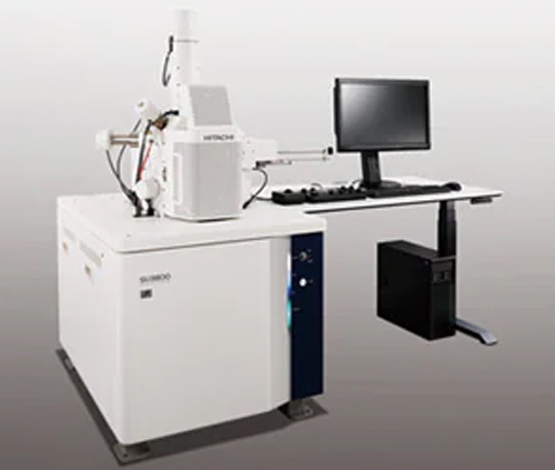
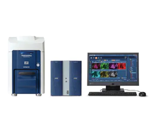
徐州Scanning electron microscope SU3800/SU3900
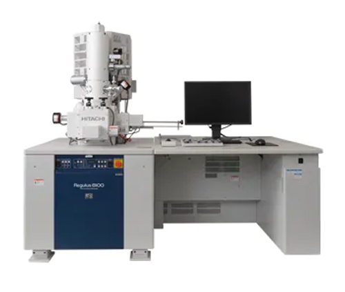
徐州Super High Resolution Field Emission Scanning Electron Microscope Regulus Series