
◆ A new standard for measuring surface topography
As the materials continue to be flattened, thinner, and finer in structure, people are beginning to require higher measurement accuracy than the traditional ordinary SPM (scanning probe microscope), stylus roughness measuring instrument, and laser microscope. Compared with the white light interference scanning microscope using the principle of optical interference, the nano-scale 3D optical interferometric measurement system VS1800 is more convenient to use, with higher measurement accuracy and larger measurement range. In addition, the traditional measurement method that uses line thickness still has major issues such as "result deviation caused by measurement position" and "result deviation caused by scanning direction". The solution of VS1800 is to calculate the parameters by referring to the surface topography evaluation method stipulated by the international standard ISO25178, and establish a new standard for measuring surface topography, which has attracted attention from all walks of life.
■Compared with ordinary measuring instruments
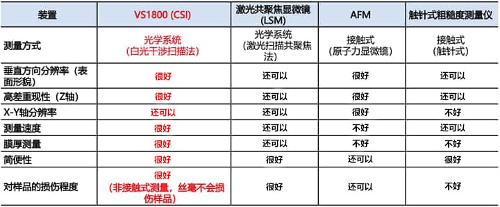
The AFM5500M nano-scale 3D probe measurement system of the atomic force microscope can also achieve a high resolution below 0.1nm. Compared with this, the major feature of the nano-scale 3D optical interferometry system VS1800 is that the measurement range in the in-plane direction is larger. Taking advantage of the respective advantages of the two measurement systems, choosing a good measurement system according to the needs is conducive to the improvement of productivity.
◆ Advantages
1. High resolution, large range
Using an original algorithm to achieve a vertical resolution of 0.01 nm (in Phase mode). Since it does not need to rely on the magnification of the objective lens to achieve high vertical resolution, even in the case of a large range (measuring field of view 6.4 mm × 6.4 mm), nano-scale roughness and height difference can be measured.
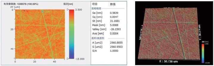
Wafer grinding surface morphology (surface roughness Sa 0.58 nm)
2. High reproducibility of measurement data
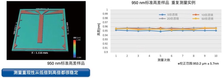
The height measurement uses interference fringes to minimize the influence of the Z drive, so that the measurement reproducibility error is less than 0.1% (in Phase mode).
3. High-speed measurement
By capturing the sample on a plane without scanning in the X and Y directions, high-speed measurement is achieved, and due to the non-contact method, it can be guaranteed that the sample will not be damaged during the measurement.
4. No damage measurement
For the measurement of foreign matter in the multilayer film structure and the inside of the multilayer film layer structure and the inside of the layer after the cross-section is formed after cutting the sample, the VS1800 can be carried out in a non-destructive manner. For the transparent layer structure sample, using the height coordinates of the lens and the reflected light generated by each interface, the virtual cross-sectional image is output through the interference fringes appearing on each optical interface.
5. Simple measurement
Equipped with an intuitively usable operation screen, you can check the processed image on the spot. You can simply list the processing and analysis content, generate the original analysis library, and reuse the analysis library. It also supports batch processing of data, unified management of multiple samples and analysis results, and alleviates complicated post-processing procedures.
In addition, the project of the international standard ISO25178 for surface topography evaluation methods is introduced, and the appropriate parameters are automatically selected for each sample. VS1800 is equipped with tools that can provide suggestions for parameter selection, which helps to improve the accuracy of management.
6. Flexible configuration
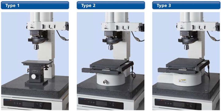
The manual XY sample stage is the basic model Type 1, and the Type 2 and Type 3 are upgraded step by step by the electric sample stage. The upgrade of each model can be carried out according to the needs, and the system can be easily introduced according to the purpose
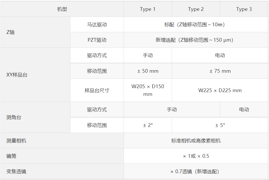
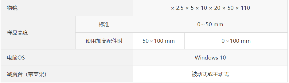
Technical index:
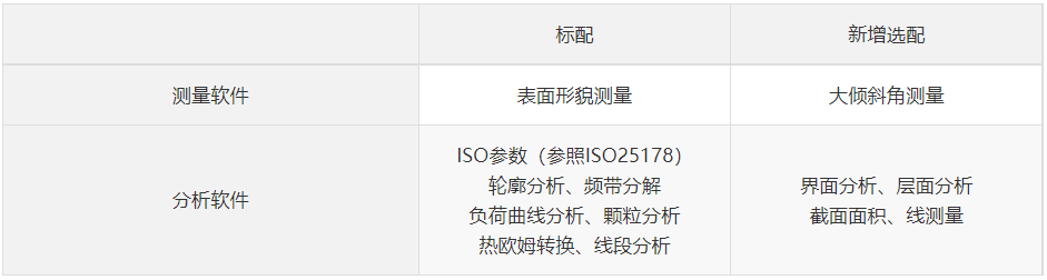
Software overview:
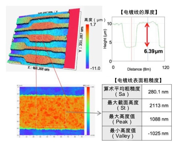
With the realization of miniaturization of various electronic parts, electroplating is becoming more and more thinner. In terms of quality management of electroplating, more precise and precise analysis methods are required. Scanning probe microscope has the characteristics of high Z-axis resolution, but on the other hand, the observation range is limited very narrow. In addition, the use of ordinary optical observation equipment can be used to observe a larger field of view, but the Z-axis resolution will be reduced.
The nano-scale 3D optical interferometry system VS1800 has both the large observation field of view in the in-plane direction and the high resolution in the height direction. Therefore, it can be used for large height difference shapes such as electroplating lines and their surface roughness. Simple and convenient measurement.
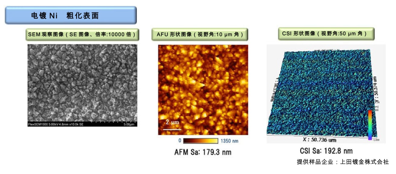
According to different purposes and purposes, surface treatment may be applied to the electroplated surface. The general surface observation method is SEM observation.
SEM images can clearly show the difference in surface properties. Generally, the information obtained by SEM is a two-dimensional image, so it is difficult to measure three-dimensional features with high accuracy.
Regarding the sample that has been roughened on the electroplated Ni surface, the results of observation and measurement using FlexSEM 1000 (SEM), AFM5500 M (AFM), and VS1800 (nano-scale 3D optical interferometry system/CSI) are shown in the figure.
Comparing the observation and measurement results of FlexSEM 1000/AFM5500 M, it can be understood that the shape observed by SEM can also see the same captured information in the AFM measurement results. In addition, it can be seen that the arithmetic average roughness Sa of AFM and CSI shows almost the same value, and the nano-scale 3D optical interferometry system can also measure the fine shapes captured by AFM. It can be seen that if AFM with high spatial resolution is used, CSI data can be cross-checked. The nano-scale 3D optical interferometric measurement system takes advantage of high-speed measurement, which is beneficial to increase the measurement speed of multiple samples. In addition, as mentioned above, by adding SEM and AFM for observation and measurement, multiple evaluations can be realized.