
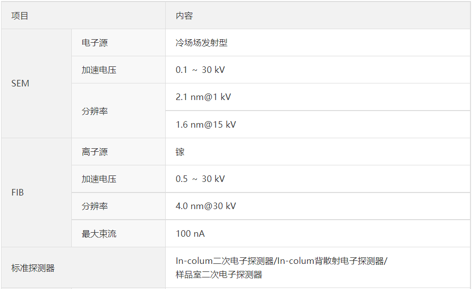
image.png SEM lens barrel and FIB lens barrel are at right angles to each other, forming the most ideal lens barrel layout for 3D structural analysis
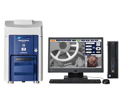
image.png Integrating a high-brightness cold-field emission electron gun and a high-sensitivity detection system, from magnetic materials to biological tissues-supporting the analysis of various samples
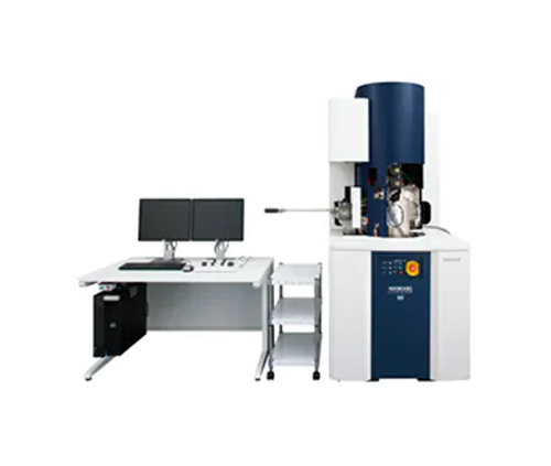
image.png By selecting the well-known Micro-sampling® system* and Triple Beam® system*, it can support the production of high-quality TEM and atom probe samples
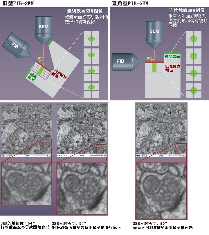
◆ SEM observation of vertical incidence cross-section can faithfully reflect the original sample structure
The SEM lens barrel and the FIB lens barrel are at right angles to each other to realize the normal incidence SEM observation of the FIB processed section.
The old FIB-SEM adopts oblique cross-section observation method, which will inevitably cause the cross-sectional SEM image to be deformed and to deviate from the field of view when collecting continuous images. The right-angle structure can avoid such problems.
By stably obtaining images that faithfully reflect the original structure, high-precision three-dimensional structure analysis is realized.
At the same time, the FIB processing section (SEM observation section) is parallel to the sample surface, which is conducive to establishing links with optical microscope images and other data.
Sample: Mouse Brain Nerve Cells
Sample source: Mr. Yoshiyuki Kubota, Institute of Natural Science Research/Institute of Physiology
◆ Cut&See/3D-EDS*1/3D-EBSD*1 can support various materials
Cut&See
From biological tissues and semiconductors to magnetic materials such as steel and nickel-support high-resolution and high-contrast observations at low acceleration voltages.
When switching between FIB processing and SEM observation, there is no need to reset conditions, and continuous images of cross-sections can be collected efficiently.

Extract cross-sectional image, 3D reconstruction image
Sample: Nickel
SEM acceleration voltage: 1 kV
Processing pitch: 20 nm
Repeat times: 675 times
3D-EDS*1
Not only supports cross-sectional SEM images, but also supports continuous collection of element distribution images of a series of cross-sections.
The optional silicon drift type large solid angle EDS detector*1 can shorten the measurement time and collect element distribution images at low acceleration voltages.

Sample: Fuel cell electrode
SEM acceleration voltage: 5 kV
Processing pitch: 100 nm
Repeat times: 212 times
Source of sample: Professor Naotake Shikayuan, Institute of Production Technology, University of Tokyo
3D-EBSD*1
Configure the SEM/FIB/EBSD detector*1 in the most ideal way to realize 3D-EBSD without moving the sample stage between FIB processing and EBSD analysis. Because there is no need to move the sample stage, the accuracy and efficiency of three-dimensional crystal orientation analysis can be greatly improved.
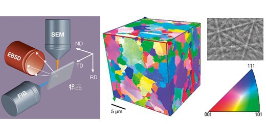
Sample: Nickel
SEM acceleration voltage: 20 kV
Processing pitch: 150 nm
Repeat times: 150 times
*1: optional
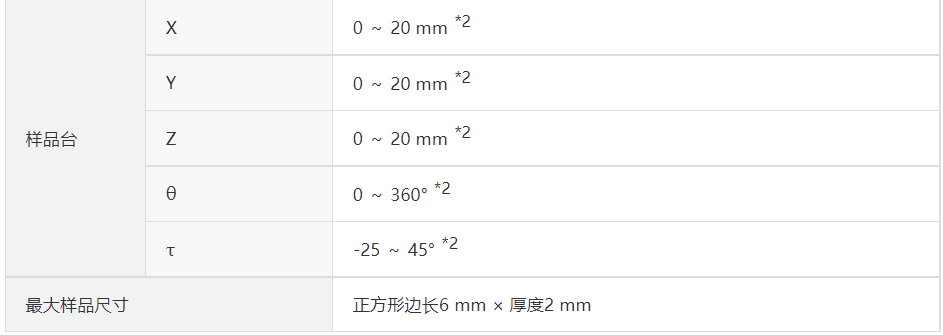
*2: The itinerary is different according to the different sample holders