
◆ Large probe current 90nA, realizing rapid processing and large area processing
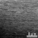
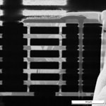
Cross-section processing of welding wire
(Processing size Width: 95µm Depth: 55µm, Processing time 20min)
◆ By improving the processing of extremely low acceleration voltage (0.5kV~) and the resolution of low acceleration voltage secondary electron image, the preparation of TEM samples with lower damage rate is realized
*1kV or less is optional
◆ Observe high-resolution SIM imaging (secondary electron imaging resolution up to 4nm@30kV)
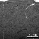
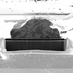
Normal part Bending part
Cross-section SIM image of aluminum can
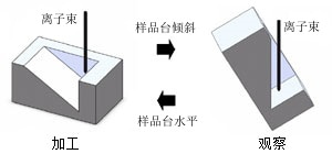
◆ Adopt high-precision 5-axis electromechanical optimal center motor platform
When the sample stage is moving (including tilting), it can automatically perform a variety of processing on multiple parts.
◆ Superior operating performance and a variety of processing modes
image.pngSection preparation program processing
image.pngTEM/STEM sample program processing
image.png automatic continuous processing
image.pngTEM sample automatic continuous finishing software
image.png bitmap processing
image.pngVector Scan processing
image.pngPreparation of nano-precision three-dimensional structure samples Other
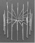
Fabrication of suspended nanowires
Sample source: Mr. Shinji Matsui, Hyogo Prefectural University
◆ SIM image 3D reconstruction analysis
Cross-section processing and cross-section observation at equal intervals are reciprocated, and multiple continuous SIM images of cross-sections can be taken, and 3D reconstruction can be carried out. From this, the three-dimensional distribution of particles and holes in the sample can be judged.
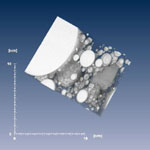
Example of analysis of filler distribution in semiconductor packaging materials
◆ Use multi-channel gas system (MGS-II) to repair the circuit
The system can be used for various purposes such as protective film materials, wiring materials, insulating films, and accelerated etching, and can be irradiated with a variety of gases.
image.png Tungsten deposition gas
image.png Platinum deposition gas
image.png Deposition gas for insulating film preparation
image.png Xenon fluoride etching gas
image.png Organic etching gas
image.png Carbon deposition gas
Machining of large depth-to-diameter ratio holes using XeF2 gas
And the use of tungsten deposited leads
◆ Rich and diverse coordinate link function
Hitachi High-Tech's original coordinate link function is rich and diverse, which can determine the correct processing position and greatly shorten the time.
image.png Link between light mirror image and SIM image
image.png Dual cursor function
image.png Japanese Patent No. 4634134 US Patent No. 7595488
image.png Establish a coordinate link with defect detection equipment
image.png The truncated wafer or chip can also establish a coordinate link with the defect detection equipment.
image.png CAD combined navigation software
image.png 4-channel gas supply system
image.png Automatic continuous processing software
image.png TEM sample automatic processing software
image.png Controller microscope other
Various options of other MI series can be selected.