
◆ Using high contrast, real-time SEM observation and processing endpoint detection functions, ultra-thin samples with a thickness of less than 20 nm can be prepared
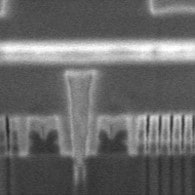
Real-time SEM observation during FIB processing *2 cases
Sample: NAND flash memory
Accelerating voltage: 1 kV
FOV: 0.6 µm
◆ The processing direction control technology (Micro-sampling®*3 system (optional) + high-precision/high-speed sample stage*) has high hopes for suppressing the curtain effect and making film samples with uniform thickness.
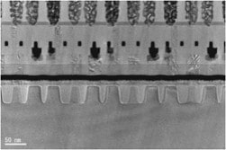
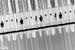
Processing direction control During normal processing
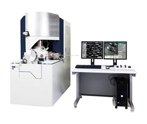
◆ Triple Beam®*1 (optional) can improve processing efficiency, and can automatically eliminate FIB damage
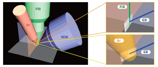
EB: Electron Beam
FIB: Focused Ion Beam (focused ion beam)
Ar: Ar ion beam
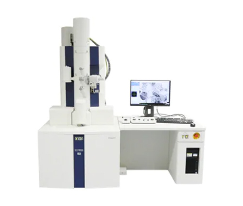
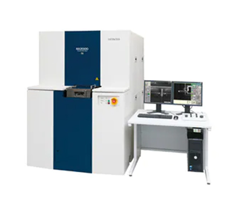
Options:
Ar/Xe ion beam system
Micro-sampling®*3 system
Defect detection equipment combined software
CAD combined navigation software
EDS (Energy Spectrometer)
TEM sample finishing wizard
TEM sample thickness management software
Continuous A-TEM
Real-time image quality optimization system
Swing processing function (for Triple Beam®*1)
Plasma cleaning machine
Vacuum transfer mechanism
Cold table