

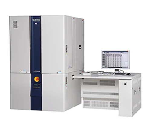
The electron microscope is a major scientific and technological invention in the 20th century. Just as the invention of the triode revolutionized the semiconductor industry, the electron microscope also greatly promoted the development of life sciences. The following editor will introduce the basic principles of Hitachi Scanning Electron Microscope.
The electron microscope is an instrument that uses electron beams and electronic lenses instead of light beams and optical lenses according to the principle of electron optics, so that the fine structure of the substance can be imaged at a very high magnification. In recent years, the research and manufacturing of electron microscopes have made great progress: on the one hand, the resolution of electron microscopes has been continuously improved. The point resolution of transmission electron microscopes has reached 0.2-0.3nm, and the lattice resolution has reached about 0.1nm. , People have been able to directly observe atomic images; on the other hand, in addition to transmission electron microscopes, a variety of electron microscopes have been developed, such as scanning electron microscopes and analytical electron microscopes.
High power microscope
1. The imaging principle of transmission electron microscope
1. Absorption image: When electrons hit the dao sample with high mass and density, the main phase formation effect is the scattering effect. Where the mass thickness of the sample is large, the scattering angle of the electrons is large, and there are fewer electrons passing through, and the brightness of the image is darker. Early transmission electron microscopes were based on this principle.
2. Diffraction image: After the electron beam is diffracted by the sample, the diffraction wave amplitude distribution at different positions of the sample corresponds to the different diffraction ability of each part of the crystal in the sample. When a crystal defect occurs, the diffraction ability of the defect part is different from that of the complete area. The amplitude distribution of the diffracted wave is not uniform, reflecting the distribution of crystal defects.
3. Phase image: When the sample is as thin as 100Å or less, electrons can pass through the sample, the amplitude change of the wave can be ignored, and the imaging comes from the change of phase.
2. Scanning electron microscope imaging principle
Scanning electron microscopes produce images of the sample surface by scanning the surface of the sample with a focused electron beam.
Electrons interact with atoms in a Hitachi scanning electron microscope sample to generate various signals that contain information about the surface mapping topography and composition of the sample. The electron beam is usually scanned in a raster scan pattern, and the position of the beam is combined with the detected signal to produce an image.
Scanning electron microscope can achieve resolution better than 1 nanometer. Samples can be observed under high vacuum, low vacuum, wet conditions (using an environmental scanning electron microscope) and a wide range of low or high temperatures.
A common scanning electron microscope mode is to detect secondary electrons emitted by atoms excited by an electron beam. The number of secondary electrons that can be detected depends on the topography of the sample and other factors.
By scanning the sample and using a special detector to collect the emitted secondary electrons, an image showing the topography of the surface is created. It can also generate high-resolution images of the sample surface, and the image is three-dimensional, to identify the surface structure of the sample.
The above content is an introduction to the basic principles of Hitachi scanning electron microscopes. Although the resolving power of electron microscopes is far better than that of optical microscopes, electron microscopes need to work under vacuum conditions, so it is difficult to observe living organisms. Irradiation can also damage biological samples.